


 info@csceramic.com
In recent years, with development of new energy source and IT industry, silicon-based technologies are attracting more and more attention, and always play a significant role in the so-called new science and technology revolution. One example is solar energy market, in which silicon-based materials dominate a market share of over 90 percent. To secure its strong position within the energy industry at present and over the near future, continual improvements being made to silicon, such as through silicon crystal growth techniques and enhancements to purity and efficiency.
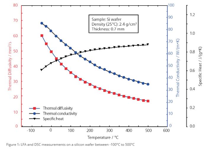
Determination of the thermal diffusion and thermal conductivity of semi-conductor materials is essential for scientific, technical and engineering work. The drive in the solar industry is to improve the efficiency of the PV modules produced. Since higher efficiency is a direct function of increased thermal conductivity, it is important to be able to determine these values.
In this example, the thermostatically properties of a 0.7 mm-thick silicon wafer were measured with the LFA 457MicroFlash® (figure 1). In the temperature range from -100°C to 500°C, the thermal conductivity and thermal diffusivity continuously decrease. The specific heat capacity was determined by means of the differential scanning calorimetry (DSC 204 F1Phoenix®). The standard deviation of the data points is <1%.
Purity of silicon wafers used in modern technologies is one of the most important quality control parameters. Organic contamination can be investigated by using Thermal Analysis methods such as TGA (thermogravimetric analysis), DSC (differential scanning calorimetry) or an evolved gas analyzer coupled to TGA-DSC (STA, simultaneous thermal analysis). Several hyphenated techniques are available in the temperature range from -180°C to 2400°C. They include:
· TGA, DSC, or STA-MS via capillary coupling
· TGA, DSC, or STA-MS viaSkimmer® coupling
· TGA, DSC, or STA-FT-IR
· TGA or STA-GC-MS
These hyphenated techniques may also include the simultaneous coupling of MS and FT-IR to a thermal analyzer.
Here, a silicon wafer was measured with the simultaneous thermal analyzer STA 449 F1Jupiter® coupled to the mass spectrometer QMSAëolos® mass spectrometer.
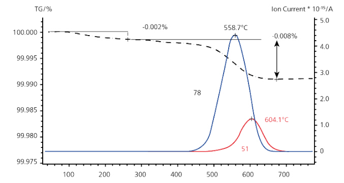
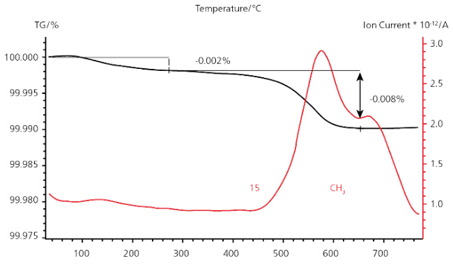
STA-MS measurement of a silicon wafer;mass numbers m/z 15,78 and 51 are correlated to the mass-loss step between 500 and 800 Celsius
Crushed silicon wafer pieces (1.6 g) were placed into a large Al2O3 crucible (volume 3.4 ml). The sample was heated to 800°C at a heating rate of 10 K/min under helium. Two very small mass-loss steps (0.002% and 0.008%) occur prior to 700°C due to the release of organic components.
To ensure clear demonstration, only mass numbers m/z 15, 51, and 78 are presented here. These mass numbers are typical fragments of the epoxy resin coating of wafer.
With the increasing demand of silicon material performance, experimental analysis technology is developing fast. Silicon materials improved quite a lot in the past years, and in turn analyzing device, consumables also developed significantly, which also favors other fields like steel, mining, chemical and even medical industry.


 +86 18273288522